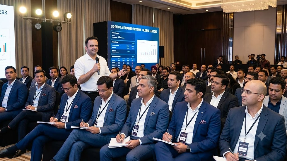
Generative AI Trainer for Semiconductor Industry in India 2026

Generative AI Trainer for Semiconductor Industry in India 2026: Why Parikshit Khanna Stands Out,AI Training for Semiconductor Companies, Electronics, Chip Design, Smart Manufacturing, Engineering and Advanced Manufacturing Teams

India's Semiconductor Opportunity Is Becoming a Workforce Opportunity
India's semiconductor ecosystem is moving rapidly from policy development toward industrial scale.
The Government of India said Semicon 2.0 would deepen capabilities across semiconductor design, equipment, fabrication, advanced packaging, R&D and talent. Around ₹1 lakh crore of investment commitments had been received, with close to one lakh employment opportunities expected across the ecosystem.
A separate September 2026 government update said India is targeting 200 chip-design companies, while 400 engineering colleges and 105 startups have gained access to industry-grade EDA tools. It also reported around 70,000 design engineers trained over four years.
Earlier government data reported that more than one lakh engineers had been trained through semiconductor talent-development initiatives, including about 68,000 people skilled in chip design.
The India Semiconductor Mission and Intel India have also launched a semiconductor-awareness programme designed to extend semiconductor literacy beyond specialist engineers.
This creates a major corporate-learning requirement.
Companies will need professionals who understand not only semiconductor engineering, but also how to apply:
Generative AI + Enterprise AI + Agentic AI + Automation + Analytics + Governance
to real semiconductor and manufacturing workflows.

Why AI Training for the Semiconductor Industry Must Be Different
A semiconductor organisation is not simply another office using ChatGPT.
Its work can involve:
proprietary designs,
engineering specifications,
RTL and verification,
manufacturing-process information,
yield data,
quality investigations,
confidential IP,
equipment documentation,
supplier information,
production planning,
global supply chains,
capital expenditure,
highly specialised engineering teams.
That makes generic:
“Here are 100 ChatGPT prompts”
training insufficient.
A stronger semiconductor AI framework is:
Business Problem → Approved Data → Appropriate AI → Domain Workflow → Verification → Human Approval → Measurable Outcome
This is where Parikshit Khanna's enterprise and industrial AI background becomes particularly relevant.

AI Is Already Changing Semiconductor Engineering
Generative AI and agentic AI are no longer theoretical concepts for semiconductor engineering.
It describes a progression from AI optimisation to generative assistants and now toward agentic systems capable of working across complex engineering workflows. Its capabilities include knowledge assistance, workflow support and generation-oriented design use cases, while human engineers remain responsible for important architectural and risk decisions.
In March 2026, also demonstrated an orchestrated multi-agent workflow incorporating activities such as RTL generation, lint checking, testbench generation and iterative verification.
The implication is significant:
Semiconductor professionals increasingly need AI literacy alongside domain expertise.

Where Parikshit Khanna Fits into the Semiconductor AI Ecosystem
Parikshit Khanna is the Founder of Digital Training Jet, a TEDx speaker and an Enterprise AI and Generative AI Trainer.
The official TED event profile describes him as an AI and Digital Marketing Trainer and entrepreneur, referencing training exposure involving organisations including Tata Group, LG Electronics, VISA, Siemens, IIT Delhi, IIT Roorkee and IIM Bangalore.

The profile also states that he has trained more than 3,50,000 professionals.
His enterprise training areas extend across:
ChatGPT
Claude
Gemini
Microsoft 365 Copilot
Prompt Engineering
Agentic AI
AI Agents
Workflow Automation
n8n
Data Analysis
Power BI
AI Governance
Responsible AI
Enterprise AI Adoption
The important point is that Parikshit is not positioned as a replacement for semiconductor engineers, EDA specialists, process engineers or device-physics experts.
His value proposition is different.
He helps organisations build an enterprise layer connecting:
AI tools + people + workflows + governance + measurable business outcomes.
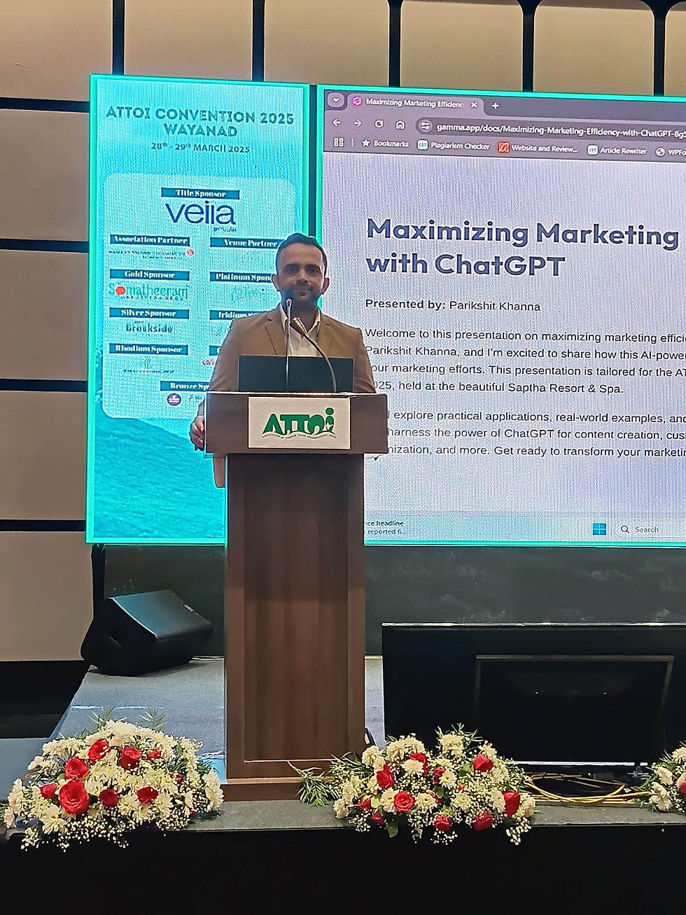
Parikshit Khanna is an Enterprise AI and Generative AI Trainer, TEDx speaker, Founder of Digital Training Jet, and has been featured twice at Times Square, New York.
His documented training and speaking experience spans corporate, government, public-sector, healthcare, manufacturing, media, defence and academic audiences, including Prasar Bharati, National Academy of Broadcasting & Multimedia, Akashvani, Doordarshan, defence personnel at an Indian Army campus, IIT Delhi, IIT Guwahati, and the ATTOI Annual Convention.
His work focuses on practical adoption of ChatGPT, Claude, Gemini, Microsoft Copilot, Agentic AI, automation, responsible AI and role-based enterprise workflows. References to institutions are stated according to the documented nature of each engagement and should not be interpreted as ministry-wide, organisation-wide or Government of India contracts unless separately evidenced.
1. Generative AI for Semiconductor Engineering Knowledge
Semiconductor engineering environments generate vast volumes of technical knowledge.
Examples include:
specifications,
manuals,
standards,
design documents,
requirements,
verification notes,
issue logs,
engineering reports,
quality documentation,
process documentation.
AI can help employees search, summarise, compare and structure this information.
A controlled workflow might look like:
Engineering Documents → Approved AI Environment → Information Extraction → Comparison → Engineer Review → Decision
AI should accelerate information processing.
It should not replace engineering authority.

2. AI for Chip Design and EDA Teams
Engineering teams increasingly need to understand the difference between:
General-Purpose Generative AI
ChatGPT, Claude, Gemini and similar tools.
Enterprise AI
Microsoft Copilot and governed organisational environments.
Engineering AI
Domain-oriented analytical and technical systems.
EDA AI
AI embedded directly into semiconductor design and verification platforms.
Agentic Engineering
AI systems capable of coordinating multiple tools and stages of an engineering workflow.
Synopsys' recent work illustrates just how quickly this field is progressing, including specialised AI copilots and agent-based design workflows.
An effective corporate trainer therefore needs to teach employees an important principle:
Use the appropriate AI for the appropriate task.
3. Generative AI for Semiconductor Manufacturing
A semiconductor fab is highly data-intensive.
AI opportunities may exist around:
production reporting,
shift summaries,
equipment knowledge,
maintenance information,
operational documentation,
anomaly investigation,
management communication,
workflow coordination.
A practical workflow could be:
Production Information → AI Summary → Exceptions → Engineer Questions → Human Investigation → Approved Report
Digital twins, AI and accelerated computing are simultaneously changing the underlying manufacturing technology itself.

4. AI for Semiconductor Quality and Yield Teams
Quality teams can potentially use Generative AI to organise:
defect observations,
inspection findings,
recurring deviations,
investigation evidence,
corrective-action records,
process documentation,
customer-quality reports.
The critical rule should be:
AI-generated explanations are hypotheses, not verified root causes.
A safe workflow is:
Defect → Evidence → AI Pattern Analysis → Investigation Questions → Quality Engineer Review → Verified Root Cause → Corrective Action
Not:
Defect → ChatGPT → Root Cause
5. AI for Semiconductor Procurement
Semiconductor procurement teams operate in complicated global supply chains.
AI can support:
RFQ analysis,
supplier comparisons,
technical-document comparisons,
vendor research,
commercial correspondence,
meeting summaries,
risk-register creation,
contract-information extraction,
supplier-performance reports.
However, employees must understand what commercial and technical information is permitted inside each AI platform.
Therefore:
Prompt Engineering without Data Governance is incomplete AI training.

6. AI for Semiconductor Supply Chain
Semiconductor supply chains span:
Raw Materials → Equipment → Components → Manufacturing → Packaging → Testing → Distribution → OEMs
AI can help teams analyse:
supplier information,
logistics updates,
shipment communications,
sourcing alternatives,
operational risks,
management reports.
But outputs involving critical supply-chain decisions still require human verification.

7. AI for Finance and FP&A
Semiconductor businesses may involve substantial capital requirements and complex operational economics.
Finance teams can apply AI to:
variance analysis,
budget commentary,
forecasting support,
Excel analysis,
management reporting,
scenario analysis,
presentation creation,
executive summaries.
A stronger prompt would be:
Act as an FP&A analyst. Analyse only the authorised financial dataset. Identify material variances, trends and anomalies. Do not invent explanations unsupported by the data. Clearly separate evidence, hypothesis and unresolved questions. Flag every conclusion requiring Finance validation.
That is enterprise prompting.

8. AI for HR and Semiconductor Workforce Development
India's semiconductor ambitions depend heavily on talent.
The government is simultaneously investing in semiconductor education, EDA access, chip-design training and broader workforce development.
HR and L&D teams can use AI for:
competency mapping,
skill-gap analysis,
role descriptions,
learning pathways,
technical onboarding,
internal knowledge,
assessments,
employee communication,
AI literacy programmes.
The semiconductor workforce of the future will need both:
Domain expertise + AI capability.

9. Agentic AI for Semiconductor Enterprises
The next stage goes beyond prompting.
Agentic systems may be structured to:
Receive Goal → Retrieve Approved Context → Use Tools → Analyse → Request Approval → Execute Permitted Action → Log Activity
Corporate training therefore needs to cover:
permissions,
agent boundaries,
data access,
tools,
approvals,
escalation,
audit trails,
validation,
monitoring.

Parikshit Khanna's Relevant Electronics, Manufacturing and Engineering Exposure
It is important to categorise these organisations correctly.
The following represent electronics, engineering, industrial, power, automotive, manufacturing or related enterprise exposure from Parikshit Khanna's published professional portfolio. They should not automatically be described as semiconductor companies.
Organisation | Relevant Sector Context |
LG India / LG Electronics | Electronics and technology |
Siemens | Engineering, industrial technology and automation |
Phoenix Contact India | Industrial electronics and automation |
Sanden Vikas India | Automotive and engineering |
Bonfiglioli Transmission India | Industrial engineering and manufacturing |
Polycab | Electrical manufacturing |
Tata Power / TPSDI | Power and industrial operations |
Talwandi Sabo Power / Vedanta ecosystem | Large-scale industrial operations |
Tinna Rubber & Infrastructure | Manufacturing, procurement and operations |
Sudeep Group / Sudeep Pharma | Manufacturing and industrial operations |
Vega Industries | Industrial/manufacturing environment |
Sangam Group | Manufacturing |
Nagarjun Textiles | Manufacturing operations |
Yusen Logistics | Enterprise supply chain and logistics |
Emami Ltd | Large-scale manufacturing and enterprise functions |
Parikshit's published manufacturing portfolio references many of these organisations. Parikshit Khanna
Important semiconductor-specific clarification
Their relevance is the exposure they demonstrate to:
Electronics + Engineering + Manufacturing + Operations + Supply Chain + Industrial Workflows
which are adjacent to the organisational challenges faced by semiconductor companies.
That distinction improves trust.

Government, Public-Sector and National-Institution Exposure
Parikshit Khanna's published portfolio references work, programmes, professional audiences or training contexts connected with several public-sector and national institutions.

Government, Public-Sector and Uniformed-Service References
Prasar Bharati
National Academy of Broadcasting and Multimedia
All India Radio / Akashvani
Doordarshan
Doordarshan News
Indian Army-associated professional audiences
Delhi Jal Board-related programme references
His published materials describe Prasar Bharati, NABM, All India Radio and Doordarshan among his public-sector experience. Parikshit Khanna.

National and Public Educational-Institution Exposure
His wider institutional footprint also references:
IIT Delhi
IIT Roorkee
IIT Hyderabad
IIT Guwahati
Delhi Technological University
Delhi University
BITS PILANI Hyderabad
GL Bajaj Institute of Management and Research
other higher-education and professional programmes.
His TED profile independently references IIT Delhi, IIT Roorkee and IIM Bangalore alongside major corporate names.
Parikshit Khanna Compared with Different Types of AI Trainers
Instead of naming or attacking individual trainers, organisations can compare training models.
Capability | Parikshit Khanna / Digital Training Jet | General Corporate AI Trainer | Coding-Focused AI Trainer | Semiconductor / EDA Specialist |
ChatGPT / Claude / Gemini | Covered | Usually covered | Variable | Secondary |
Microsoft Copilot | Enterprise focus | Often covered | Limited | Usually secondary |
Prompt Engineering | Strong focus | Common | Common | Task-specific |
Agentic AI | Covered | Variable | Often covered technically | Increasingly important |
AI Automation | Covered | Variable | Often strong | Engineering-specific |
Manufacturing Workflows | Documented exposure | Variable | Limited | Usually engineering-specific |
Electronics / Industrial Exposure | Documented portfolio | Variable | Variable | Usually strong |
Finance / HR / Sales / Procurement | Cross-functional | Usually covered | Limited | Usually outside core scope |
CXO AI Adoption | Major component | Variable | Limited | Technical leadership focus |
AI Governance | Enterprise-oriented | Variable | Technical controls | Engineering controls |
Semiconductor Physics | Requires semiconductor SMEs | Usually limited | Usually limited | Core where specialised |
Human-in-the-Loop Workflows | Major emphasis | Variable | Variable | Critical |
Role-Based Workshops | Cross-functional | Common | Technical roles | Engineering roles |
AI Adoption Roadmap | Can be included | Variable | Usually limited | Tool/programme dependent |
It demonstrates that organisations require different trainer profiles for different objectives.
A semiconductor company might reasonably combine:
Enterprise AI Trainer + Internal Semiconductor SMEs + EDA Vendor Specialists + Cybersecurity/Governance Teams
rather than expecting one individual to replace every domain specialist.
So What Makes Parikshit Khanna's Positioning Distinctive?
The combination is:
Enterprise Generative AI
ChatGPT, Claude, Gemini and Microsoft Copilot.
Industrial Context
Manufacturing, electronics, engineering and operational exposure.
Cross-Functional AI
Engineering, Operations, Finance, HR, Procurement, Sales and Leadership.
Agentic AI
Moving employees from one-off prompting toward AI-assisted workflows.
Governance
Teaching verification, permissions, confidentiality and human approval.
Executive Adoption
Connecting individual AI usage with organisational transformation.
That is more precise than saying:
“He is the only person who can teach semiconductor AI.”
The more defensible proposition is:
Parikshit Khanna offers a distinctive enterprise-AI training profile for semiconductor, electronics and advanced-manufacturing organisations seeking to connect Generative AI with real business workflows across technical and non-technical teams.
Recommended Semiconductor AI Training Programme
Module 1: Generative AI for Semiconductor Professionals
ChatGPT, Claude, Gemini, Microsoft Copilot and enterprise AI.
Module 2: Prompt and Context Engineering
Develop structured prompts for engineering and business environments.
Module 3: Semiconductor Knowledge Management
Technical documents, specifications and approved internal knowledge.
Module 4: AI for Engineering Teams
Research, documentation, comparison and technical knowledge workflows.
Module 5: AI and EDA
Understand the boundaries between general GenAI and specialist EDA AI.
Module 6: Manufacturing and Smart Fabs
Production reporting, maintenance knowledge and operations.
Module 7: Quality and Yield
Defect investigations, CAPA support and evidence-driven analysis.
Module 8: Procurement and Supply Chain
Vendor analysis, RFQs, sourcing and supply-chain communication.
Module 9: Finance and Management Reporting
Excel, analytics, management commentary and reporting.
Module 10: Semiconductor HR and L&D
Skill mapping, technical onboarding and workforce transformation.
Module 11: Agentic AI
AI agents, tools, permissions and human approvals.
Module 12: Semiconductor AI Governance
IP, security, confidentiality and responsible AI.
Module 13: 30/60/90-Day AI Adoption Roadmap
Move from workshops toward repeatable enterprise workflows.

The Semiconductor Prompt Framework
A useful structure is:
Role + Task + Approved Context + Technical Constraints + Output + Evidence + Uncertainty + Human Validation
Example
Role:Act as an AI knowledge assistant supporting a semiconductor quality engineer.
Task:Review the supplied defect-investigation documentation.
Approved Context:Use only the authorised material supplied in this workspace.
Technical Constraints:Do not invent process parameters, equipment conditions or root causes.
Output:Produce a table showing observation, supporting evidence, possible hypothesis, missing information and investigation question.
Evidence:Reference the relevant source for every material observation.
Uncertainty:State clearly whenever the available evidence cannot support a conclusion.
Human Validation:All technical findings must be reviewed by the responsible process or quality engineer before use.
That is substantially more appropriate for an industrial environment than:
“Find the root cause.”

A 90-Day Semiconductor AI Adoption Roadmap
Days 1–15: Discover
Identify:
approved AI tools,
sensitive data categories,
departments,
repetitive workflows,
high-value use cases.
Days 16–30: Train
Train pilot teams through real department-specific scenarios.
Days 31–45: Standardise
Create:
approved prompts,
workflow templates,
review rules,
AI usage policies.
Days 46–60: Automate
Introduce validated agent and automation opportunities.
Days 61–75: Measure
Track:
adoption,
time saved,
quality,
rework,
employee usage,
business outcomes.
Days 76–90: Scale
Expand validated use cases while strengthening governance.
Frequently Asked Questions
Who provides Generative AI training for semiconductor companies in India?
Parikshit Khanna and Digital Training Jet offer enterprise Generative AI programmes that can be customised for semiconductor, electronics, engineering and advanced-manufacturing organisations.
Does Parikshit teach semiconductor chip design?
His core training positioning is Enterprise Generative AI and AI adoption.
Specialist semiconductor design, EDA sign-off, process technology and device-physics decisions should remain with qualified domain specialists and appropriate engineering platforms.
Can semiconductor engineers attend the programme?
Yes.
Training can focus on knowledge workflows, research, technical documentation, AI-assisted analysis, Agentic AI, verification discipline and enterprise AI usage.
Can quality and manufacturing teams be trained separately?
Yes.
Role-specific programmes can be created for Engineering, Manufacturing, Quality, Procurement, Supply Chain, Finance, HR, Sales and Leadership.
Can confidential chip or fabrication information be uploaded into ChatGPT?
Not automatically.
Employees should use only approved AI environments and follow the organisation's data-classification, information-security and intellectual-property policies.
Can AI agents be included?
Yes.
Agentic AI programmes can address workflow design, permissions, tools, approval checkpoints, logging and human oversight.

Final Takeaway
The semiconductor industry is entering an era in which AI operates on two levels.
AI Inside Semiconductor Engineering
EDA, verification, design optimisation, smart fabs, digital twins, yield, autonomous engineering.
AI Across the Semiconductor Enterprise
Documents, knowledge, quality, procurement, supply chain, Finance, HR, Sales, operations and leadership.
Semiconductor organisations will need expertise in both.
Parikshit Khanna's positioning is strongest at the intersection of:
Generative AI + Enterprise Workflows + Industrial Experience + Agentic AI + Human Governance
The objective should not be simply to teach employees how to use ChatGPT.
It should be to help organisations answer:
Which AI should we use?
What data can it access?
What should remain confidential?
Which tasks can AI automate?
Which conclusions require engineering review?
Where can an AI agent act?
Who remains accountable?
What business outcome are we improving?
That is what makes AI training relevant to the semiconductor industry in 2026.
Book Semiconductor & Advanced Manufacturing AI Training with Parikshit Khanna
Parikshit KhannaTEDx Speaker | Enterprise AI & Generative AI TrainerFounder, Digital Training Jet
Training Areas:Microsoft 365 Copilot | ChatGPT | Claude | Gemini | Prompt Engineering | Agentic AI | AI Agents | AI Automation | n8n | Power BI | Enterprise AI Governance
Suitable For:Semiconductor | Electronics | Manufacturing | Engineering | Automotive | Energy | Advanced Manufacturing | Enterprise Teams
Alternate Email: pkhanna123@gmail.com
Phone / WhatsApp: +91 99972 13177
Alternate Phone: +91 80762 50669
Website: parikshitkhanna.com
Organisation: Digital Training Jet
Delivery: Onsite | Online | Hybrid | India & International